As I had been sketching the slow start and rectification in my CAD schematics editor, I started with the board layout immediately when I felt that the design was completed.
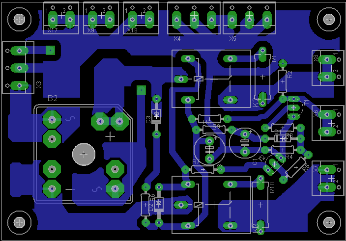
There were no considerations of great importance for the layout, other than perhaps:
- Very thick PCB tracks were used for the V+/V- rails
- A rough star-ground point with 6 connection screw-terminals was created
- Connections for the return ground of the reservoir capacitors were added separate from the star-ground (closer to the mains ground), to avoid the charging currents from producing harmful voltage noise.
The finished PCB looks like this:
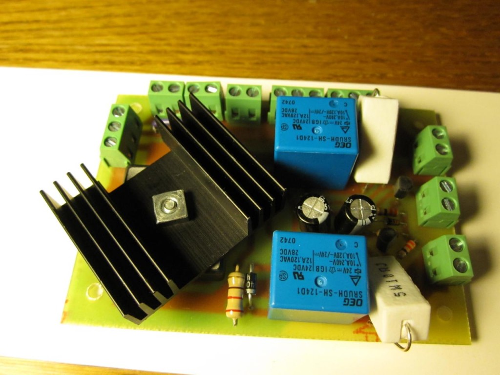
Etching of the board was done using homemade equipment, and the resulting board, complete with mounted components, is shown below:
Note: The extra heatsink on top of the rectifier bridge was probably not necessary, I just added it because it looked neat 😉 It’s originally intended for use against a TO-220 transistor.
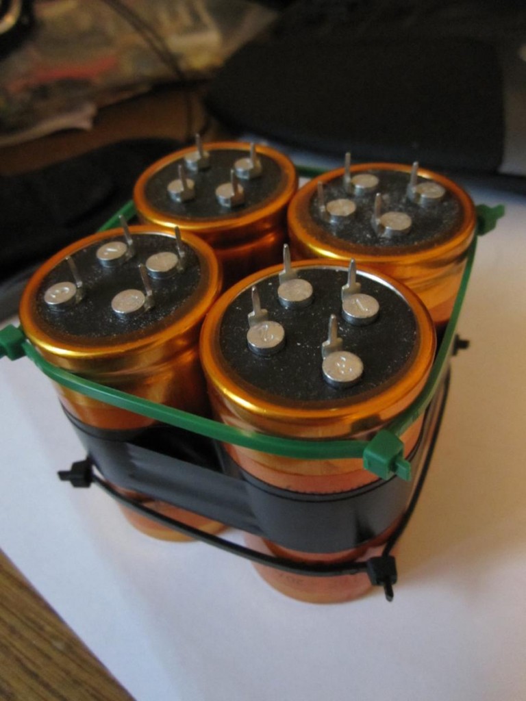
The capacitor bank was assembled, two caps for each supply rail:
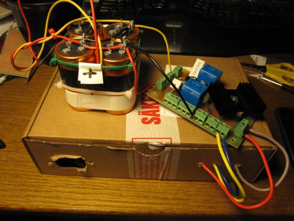
 The mains transformer, complete with mains connector and slow-blow fuse were connected together in a paper box housing. This obviously will not pass any kind of security standard ever, and was only intended as temporary housing during my laborations with the circuit, in order to avoid any accidental touching of high-voltage wires.
At first try, the core PSU circuitry worked fine, but the slow-start circuit did not switch the relays. Some measuring showed that the RC-node used in the slow-start timing circuitry only reached 18.4 V, which would only give 0.4 V of base voltage to the transistor, never turning them on. A fix to this was to solder a resistor in parallel with the resistor in the RC-link to decrease the voltage drop over it. The fix worked and the relays clicked after roughly one second as planned.
I performed some very simple tests:
- Measured supply rails first to see if voltage levels looked correct. They showed roughly +-33 V as expected.
- Connected a 68R heatsinked resistor between V+ and ground. The resistor would draw a current of
. V+ only moved by slightly less than volt or so during this, when measuring DC voltage with a multimeter, which is fine.
- Connected two MOSFETS and an LED to the muting output, to make sure that the mute circuitry seemed to work as planned (which it did.)
Better testing would perhaps be to look at the waveforms in an oscilloscope. This is not entirely interesting for this circuit though, as the PSU is unregulated and not meant to be nice looking. The amplifier circuitry will have high PSRR anyway.


