With the circuit board completed, I plugged it into my +-35 V supply for testing. I put a 1 kHz sine-wave generator at the input and looked at the output with an oscilloscope. I saw a good looking sine-wave at the output, and it seemed the circuit was working fine. That’s when I made the mistake of increasing the level of the input source to see what clipping would look like at the output. Instead of any neat waveform phenomena on the oscilloscope, I instead got to see the transistors of the voltage-amplification stage burn out.
I was hoping this was just a one time occurance, so I soldered off the transistors and replaced them with new ones, but the exact same thing happened when powering the circuit again. This time however, I had the input grounded! The only conclusion I could draw from this was that the first failure had destroyed/altered other components in a more subtle way than burning them outright. So, this chapter is about the troubleshooting process of this circuit failure!
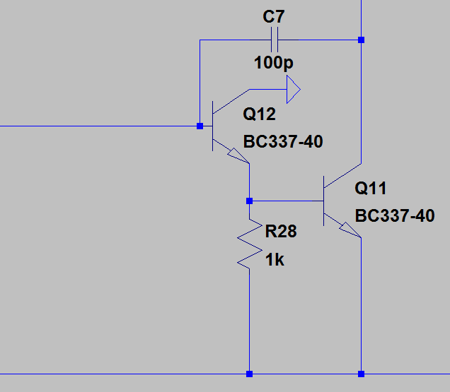
 In this image we see the transistors of the VAS-stage. In the initial circuit failure, the Q11 transistor burned out completely.
Problem 1: Where did the destructive current come from?
I looked at the collector path to V+ from the transistor in the schematic and noted that it was not very low-impedance and probably could not source the excessive current needed to destroy the transistor.
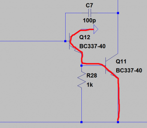
A much more likely candidate is the following path:
 If the Q12 transistor for some reason turns on completely and shorts out emitter and collector, the ground node will see a diode connection to V- through the P-N junction of the Q11 transistor, and a very large current will flow, ultimately destroying the base-emitter region of the transistor. Q12 would not burn out as easily (or at least not as visibly) as Q11 since a collector-emitter voltage can be cut down to about 0.1-0.2V by the transistor and can present a much lower impedance in comparison to the base-emitter diode of Q11.
Next, I connected the amplifier to my +-12V supply and limited the current to 150 mA. After some measurements it was clear that something was wrong with Q12 as well. Both the base and emitter nodes were sitting at -0.8 V (note, the current limiting put the V- voltage at about -1.75 V). I turned off the supply and tried measuring the diode from base to collector, and could not see any diode voltage on my multimeter. Time to replace Q12 as well!
While replacing Q12, I took the liberty of adding a 1k ohm resistor between the collector and V+ to limit the current, in order to make troubleshooting a bit easier. And strangely enough, the entire circuit started working after this. It can’t just have been the two transistors being replaced (since I already tried that before burning them a second time). So now that everything works, it will unfortunately be much harder to figure out the mechanism causing Q12 to conduct overtly much if there is nothing there to limit the current.
